Staying on an older node might ensure AMD the production capacity they need/want/expect. If they had aimed for the latest 3nm then they'd have get in line behind Apple and Nvidia. That would be my guess, why aim for 3nm, if you can't get fab time and you're still gaining a 15% speed increase.
It's the GPUs that are just getting increasing inaccessible, price wise.
A decade ago, Steam's hardware survey said 8GB was the most popular amount of RAM [1] and today, the latest $1600 Macbook Pro comes with.... 8GB of RAM.
In some ways that's been a good thing - it used to be that software got more and more featureful/bloated and you needed a new computer every 3-5 years just to keep up.
[1] https://web.archive.org/web/20140228170316/http://store.stea...
I guess you _can_ game on those 2 CU GPUs, but it really doesn't seem to be intended for that.
Not sure that I actually CAN. 56 GHz is already a lot.
Faster GPU is reserved for APUs. These graphics are just here for basic support.
https://www.anandtech.com/show/21419/amd-announces-the-ryzen...
The GPU on these parts is there mostly for being able to boot into BIOS or OS for debugging. Basically when things go wrong and you want to debug what is broken (remove GPU from machine and see if things work)
This could be a thing if you're running native Linux but some games only work on Windows which you run in a VM instead of dual booting.
That's wildly not true. Transcoding, gaming, multiple displays, etc. They are often used as any other GPU would be used.
Not at all. I drive a 38" monitor with the iGPU of the 7700X. If you don't game and don't run local AI models it's totally fine.
And... No additional GPU fans.
My 7700X build is so quiet it's nearly silent. I can barely hear it's Noctua NH-12S cooler/fan ramping up when under full load and that's how it should be.
You're misguided.
Apple has excellent Notebook CPUs. Apple has great IPC. But AMD and Intel have easily faster CPUs.
https://opendata.blender.org/benchmarks/query/?compute_type=...
Blender Benchmark
      AMD Ryzen 9 7950X (16 core)         560.8
      Apple M2 Ultra (24 cores)           501.82
      Apple M3 Max (12 cores)             408.27
      Apple M3 Pro                        226.46
      Apple M3                            160.58
I'm a software developer using a compiler that 100%s all cores. I like fast multicore.
      Apple Mac Pro, 64gb, M2 Ultra, $7000
      Apple Mac mini, 32gb, M2 Pro, 2TB SSD, $2600
[Edit] Made a c&p mistake, the mini has no ultra.
I know that there's some work happening about UEFI+ARM (https://developer.arm.com/Architectures/Unified%20Extensible...), but its support is very rare. The only example I can recall is Ampere Altra: https://www.jeffgeerling.com/blog/2023/ampere-altra-max-wind...
I expect that this will remain true for Zen 5 and the next Intel CPUs.
The only important differences in throughput between Intel and AMD were for the 512-bit load and store instructions from the L1 cache and for the 512-bit fused multiply-add instructions, where Intel had double throughput in its more expensive models of server CPUs.
I interpret AMD's announcement that now Zen 5 has a double transfer throughput between the 512-bit registers and the L1 cache and also a double 512-bit FP multiplier, so now it matches the Intel AVX-512 throughput per clock cycle in all important instructions.
Except for the fact that Intel hasn't had any AVX-512 for years already in consumer CPUs, so there's nothing to compare against really in this target market
Not exactly related, but AMD also has a much better track record when it comes to speculative execution attacks.
Having all 512-bit pipes would still be a massive throughput improvement over Zen 4 (as long as pipe count is less than halved), if that is what Zen 5 actually does; things don't stop at 1 op/cycle. Though a rather important question with that would be where that leaves AVX2 code.
A 50% speed boost would probably make the CPU option a lot more viable for home chatbot, just due to how easy it is to make a system with 128gb RAM vs 128gb VRAM.
I personally am going to experiment with the 48gb modules in the not too distant future.
The thing discussed is that Zen 4 does 512-bit SIMD ops via splitting them into two 256-bit ones, whereas Zen 5 supposedly will have hardware doing all 512 bits at a time.
128GB isn't exactly a lot, so that would surprise me if it wasnt supported.
Which website is that?
With LLMs, I feel like the line between consumer and professional is getting blurred.
Not that CPU is really reasonable for LLMs that big...
Sooner or later, AI will need to run on the edge, and that'll require RAM bandwidths measured in multiple terabytes per second, as well as "tensor" compute integrated closely with CPUs.
Sure, a lot of people see LLMs as "useless toys" or "overhyped" now, but people said that about the Internet too. What it took to make everything revolve around the Internet instead of it being just a fad is broadband. When everyone had fast always-on Internet at home and in their mobile devices, then nobody could argue that the Internet wasn't useful. Build it, and the products will come!
If every gaming PC had the same spec as a GB200 or MI300, then games could do real-time voice interaction with "intelligent" NPCs with low latency. You could talk to characters, and they could talk back. Not just talk, but argue, haggle, and debate!
"No, no, no, the dragon is too powerful! ... I don't care if your sword is a unique artefact, your arm is weak!"
I feel like this is the same kind of step-change as floppy drives to hard drives, or dialup or fibre. It'll take time. People will argue that "you don't need it" or "it's for enterprise use, not for consumers", but I have faster Internet going to my apartment than my entire continent had 30 years ago.
"AI will need to run..."
Let's wait and see what actually happens to AI before being too eager to change the design of computers. I'm also pretty sure there will be a better solution than what you described.
While I’m totally one of those people, aren’t we some rather small minority, nowadays? I mean, obviously still big enough for companies to produce parts we want, but I always keep reading how more and more people are using laptops instead of desktops.
I want plot/character driven games like RPGs to be a curated & carefully designed, plotted, and paced experience.
I want speech & narrative to be scripted! It means someone sat down and thought about the experience it produces for the player. It means a real voice actor has performed it, putting the right emotion and pacing into the line.
I don't want AI generated stilted dialogue, uncanny valley speech, etc.
And I also don't want an extra few hundred watts of power draw on gaming PCs - they're already high and in modern games the CPU is under pretty substantial load, the GPU is maxed out, and the GPU's AI/NPU style cores are being used for things like DLSS too.
Bringing in more compute resource for running speech to text, LLMs, text to speech, etc fast enough to not feel horrible is going to come at substantial power and financial cost.
I've seen this line pulled out before and it always seems like an assumption than actual reality.
Anyone know if the 'strix' apu thing is expected to be a ddr-on-package or still using with separate sticks? Search engine is not going well for me.
Sure, you can always find naysayers about any tech, but we've also seen plenty of useless toys, so that internet fact doesn't help your argument that AI will come to the edge in any way (and no, email was not a fad even at dial-up speeds, so you don't even have the internet fact)
If so, is this unique - that a whole industry of relies on one company?
Nvidia 30-series was fabbed by Samsung.
So there is some competition in the high-end space, but not much. All of these companies rely on buying lithography machines from ASML, though.
Isn't Lunar Lake made by TSMC? Supposedly they have comparable efficiency to AMD/Apple/Qualcomm at the cost of making their fab business even less profitable
Because the US will defend Taiwan.
The article makes it appear as:
* 16x PCIe 5.0 lanes for "graphics use" connected directly to the 9950X (~63GB/s).
* 1x PCIe 5.0 lane for an M.2 port connected directly to the 9950X (~4GB/s). Motherboard manufacturers seemingly could repurpose "graphics use" PCIe 5.0 lanes for additional M.2 ports.
* 7x PCIe 5.0 lanes connected to the X870E chipset (~28GB/s). Used as follows:
  * 4x USB 4.0 ports connected to the X870E chipset (~8GB/s).

  * 4x PCIe 4.0 ports connected to the X870E chipset (~8GB/s).

  * 4x PCIe 3.0 ports connected to the X870E chipset (~4GB/s).

  * 8x SATA 3.0 ports connected to the X870E chipset (some >~2.4GB/s part of ~8GB/s shared with WiFi 7).

* WiFi 7 connected to the X870E chipset (some >~1GB/s part of ~8GB/s shared with 8x SATA 3.0 ports).Typical use cases and motherboards give an x16 slot for graphics, x4 each to at least one or two M.2 slots for SSDs, and x4 to the chipset. Last generation and this generation, AMD's high-end chipset is actually two chipsets daisy-chained, since they're really not much more than PCIe fan-out switches plus USB and SATA HBAs.
Nobody allocates a single PCIe lane to an SSD slot, and the link between the CPU and chipset must have a lane width that is a power of two; a seven-lane link is not possible with standard PCIe.
Also, keep in mind that PCIe is packet-switched, so even though on paper the chipset is over-subscribed with downstream ports that add up to more bandwidth than the uplink to the CPU provides, it won't be a bottleneck unless you have an unusual hardware configuration and workload that actually tries to use too much IO bandwidth with the wrong set of peripherals simultaneously.
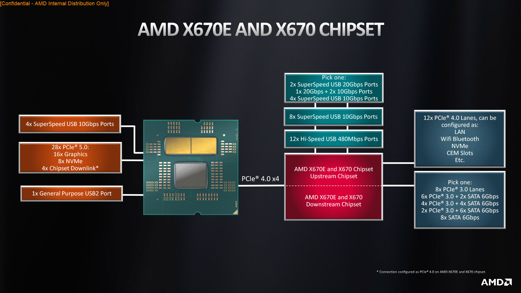
Block diagram for AM5 (X670E/X670): https://www.techpowerup.com/review/amd-ryzen-9-7950x/images/...
Block diagram for AM4 (X570): https://www.reddit.com/r/Amd/comments/bus60i/amd_x570_detail...
However you are right that such a choice is very unlikely for computers using AMD CPUs or Intel Core CPUs.
https://www.anandtech.com/show/20057/amd-releases-epyc-8004-...
2011/2011-3/2066 were actually a reasonable size. Like LGA3678 or whatever as a hobbyist thing doesn't seem practical (the W-3175X stuff) and that was also 6ch, and Epyc/TR are pretty big too etc. There used to exist this size-class of socket that really no longer gets used, there aren't tons of commercial 3-4-6 channel products made anymore, and enthusiast form-factors are stuck in 1980 and don't permit the larger sockets to work that well.
The C266 being able to tap off IOs as SAS3/12gbps or pcie 4.0 slimsas is actually brilliant imo, you can run SAS drives in your homelab without a controller card etc. The Asrock Rack ones look sick, EC266D4U2-2L2Q/E810 lets you basically pull all of the chipset IO off as 4x pcie 4.0x4 slimsas if you want. And actually you can technically use MCIO retimers to pull the pcie slots off, they had a weird topology where you got a physical slot off the m.2 lanes, to allow 4x bifurcated pcie 5.0x4 from the cpu. 8x nvme in a consumer board, half in a fast pcie 5.0 tier and half shared off the chipset.
https://www.asrockrack.com/general/productdetail.asp?Model=E...
Wish they'd do something similar with AMD and mcio preferably, like they did with the GENOAD8X. But beyond the adapter "it speaks SAS" part is super useful for homelab stuff imo. AMD also really doesn't make that much use of the chipset, like, where are the x670E boards that use 2 chipsets and just sling it all off as oculink or w/e. Or mining-style board weird shit. Or forced-bifurcation lanes slung off the chipset into a x4x4x4x4 etc.
https://www.asrockrack.com/general/productdetail.asp?Model=G...
All-flash is here, all-nvme is here, you just frustratingly can't address that much of it per system, without stepping up to server class products etc. And that's supposed to be the whole point of the E series chipset, very frustrating. I can't think of many boards that feel like they justify the second chipset, and the ones that "try" feel like they're just there to say they're there. Oh wow you put 14 usb 3.0 10gbps ports on it, ok. How about some thunderbolt instead etc (it's because that's actually expensive). Like tap those ports off in some way that's useful to people in 2024 and not just "16 sata" or "14 usb 3.0" or whatever. M.2 NVMe is "the consumer interface" and it's unfortunately just about the most inconvenient choice for bulk storage etc.
Give me the AMD version of that board where it's just "oops all mcio" with x670e (we don't need usb4 on a server if it drives up cost). Or a miner-style board with infinite x4 slots linked to actual x4s. Or the supercarrier m.2 board with a ton of M.2 sticks standing vertically etc. Nobody does weird shit with what is, on paper, a shit ton of pcie lanes coming off the pair of chipsets. C'mon.
Super glad USB4 is a requirement for X870/X870E, thunderbolt shit is expensive but it'll come down with volume/multisourcing/etc, and it truly is like living in the future. I have done thunderbolt networking and moved data ssd to ssd at 1.5 GB/s. Enclosures are super useful for tinkering too now that bifurcation support on PEG lanes has gotten shitty and gpus keep getting bigger etc. An enclosure is also great for janitoring M.2 cards with a simple $8 adapter off amazon etc (they all work, it's simple physical adapater).
But now I'm seeing lots of things I'm locked out. Faster ethernet standards, the fun that brings with tons of GPU memory (no USB4, can't add 10Gbe either), faster and larger memory options, AV1 encoding. It's just sad that I bought a laptop right before those things were released.
Should had go with a proper PC. Not doing this mistake anymore.
Yea closest I see to being better about it is Frame.work laptops, and even then it's not as good a story as desktops, just the best story for upgrading a laptop right now. Other than that buying one and making sure you have at least two thunderbolt (or compatible) ports on separate busses is probably the best you can do since that'd mean two 40Gb/s links for expansion even if it's not portable, but would let you get things like 10GbE adapters or fast external storage and such without compromising too much on capability.
https://x.com/msigaming/status/1793628162334621754
Hopefully won't be too long now.
The mobile APUs are way more interesting.
Interestingly though the 9700X seems to be rated at 65W TDP (compared to a 105 TDP for the 7700X). I run my 7700X in "eco mode" where I lowered the TDP to max 95 W (IIRC, maybe it was 85 W: I should check in the BIOS).
So it looks like it's 15% overall more power with less power consumption.
9700x runs 100MHz higher on the same process as the 7700x. If they are actually running at full speed, I don't see how 9700x could possibly be using less power with more transistors at a higher frequency. They could get lower power for the same performance level though if they were being more aggressive about ramping down the frequency (but it's a desktop chip, so why would they?).
Strix Halo appears to be AMD's competitor to Apple SoCs which will feature a much bigger iGP and much greater memory bandwidth. When we hear more about that, comparisons will be apt.
For me as a developer Geekbench Clang benchmarks:
    M2 Ultra   233.9 Klines/sec
    7950x      230.3 Klines/sec
    14900K     215.3 Klines/sec
M3 Max 196.5 Klines/secNot a fair comparison. If we're on about Geekbench as per the announcement, it's +35%. The 15% is a geomean. It might not be better but definitely not far off Apple.
In a similar manner, except Geekbench the geomean of M3 vs M4 isn't that great either.
It will be significantly slower in ST than M4, and even more so against the M4 Pro/Max.
AMD claims +35% IPC improvements in that specific benchmark, due to improvement in the AVX512 pipeline.
Overall GB6 improvement is likely around 10-15% only because that's how much IPC improved while clock speed remains the same.
The real issue is that most code people run doesn't use very much SIMD and even less uses AVX-512.
It's disappointing because M4 is significantly ahead. I would expect Zen to make a bigger leap to catch up.
Also, this small leap opens up for Intel's Arrow Lake to take the lead.
It's as if our planet wasn't being destroyed at a frightening speed. We're headed towards a cliff, but instead if braking, we're accelerating.
A 7950X in Eco mode is ridiculously capable for the power it pulls but that's less of a selling point.
That's why undervolting has become a thing to do (unless you're an Intel CPU marketer) - give up a few percent of your all-core max clock rate and cut your wattage used by a lot.
anything else will require newer SOCKET, MB AND RAM
Question: Am I understanding this correctly that AMD will be using a node size from TSMC that’s 2-years old, but in a way it’s kind of older.
Because N4 was like a “N5+” (and the current gen is “N3+”).
EDIT: why the downvotes for a question?
I am personally very curious how it compares vs Intel's 15th gen, which is rumored to be on Intel 20 process.
In light of the "very good but not incredible" generation-over-generation improvement, I guess we can now play the "can you get more performance for less dollars buying used last-gen HEDT or Epyc hardware or with the newest Zen 5 releases?" game (NB: not "value for your dollar" but "actually better performance").
But I am more interested in the cleanup of the GPU hardware interface (it should be astonishingly simple to program the GPU with its various ring buffers, like as it is rumored to be the case on nvidia side) AND in the squishing of all hardware shader bugs: look at valve ACO compiler erratas in mesa, AMD hardware shader is a bug minefield. Hopefully, the GFX12 did fix ALL KNOWN SHADER HARDWARE BUGS (sorry, ACO is written with that horrible c++, I dunno what went thru the head of valve and no, rust syntax is a complex as c++, then this is toxic too).