Continuing the well established trend of making bold claims about physical dimensions that have nothing to do with any of the structures in the chip, and the name scales better than the tech.
What they actually deliver is a "nanostack architecture" built with ~5nm features that according to them is comparable to a hypothetical real sub-1nm chip.
It's an impressive achievement nonetheless but it looks like the industry has a few too many marketers.
For silicon, the gate length of a FET has a lower limit somewhere between 10 nm and 15 nm.
The current CMOS manufacturing processes have not reached the limit yet. For making smaller transistors, a transition to other semiconductor materials will be necessary.
The vertical thicknesses of various layers may be of only a few nanometers or even of a fraction of a nanometer, but that does not matter directly for the circuit density.
The supposed node size refers to horizontal dimensions, not to vertical dimensions.
Vertical dimensions of around 1 nanometer or less could be achieved already many decades ago, because they depend on growth speed and on time, not on lithography, like the horizontal dimensions.
The industry should have stopped decades ago to talk about the "size" but they should have characterized a CMOS process by its density, e.g. in logic gates per square mm.
However, an actual concrete number would be disliked by marketing, because they could no longer claim that their "1 nm" process is better than the "2 nm" process of another vendor, if their density is not really better.
We should flip the transistors sideways then!
"You can't go to the sun! You'll burn alive!"
"Duh! That's why we're going at night!"
How would you fix that? This is a global scam. Big Markets regulating them: that would have to be the USA and EU.
It describes density measure where you can compare it to planar transistors from the 28-nanometer (28 nm) node around 2010 to 2011 and before. A "0.7 nm" node has equivalent transistor density as if we could have shrunk standard flat transistor node down to 0.7 nanometers.
MTr/mm = 0.6×(NAND2 Tr Count)/(NAND2 Cell Area) + 0.4×(Scan Flip Flop Tr Count)/(Scan Flip Flop Cell Area)
If you want to reduce "effectiveness" of some process down to a single number, then density is far from the worst metric to pick.
mass per volume is one example.
Sometime around 2011 when Intel named their process node 22nm which the gate length was 26nm
I know they won't go for an anything that makes as much sense as 5nm3, so I vote for "1nm hyper space"
Different companies measure it differently too. This was a while ago, but I remember reading that Intel 10nm was more or less close to TSMC 7nm. I'm sure this is still true to varying degrees.
We care about PPA (power, performance, area) and not how large or not-large features actually are. Comparing gate lengths between a 1980s planar transistor and a 2010s 3D FinFET or GAA transistor is obviously nonsense, the relatively aligned node names of the industry actually do make sense as a shortcut here.
Is there a limit to how small things can go? A single atom?
Is there a physical/molecular limit to Moore's Law?
Once you make the gate of a transistor small/thin enough, quantum effects take over. Electrons will randomly teleport into and through the gate causing the transistor to conduct when it shouldn't. I don't have numbers to hand, but it's on the order of a few atoms wide. There's really nothing that can be done about it either, as far as we know. Electrons just aren't physical objects at this scale, you can't simply exclude them from any given volume of space. The electron wave function will simply just appear wherever it wants (within the electron probability cloud). The only way to stop it is to make your insulating junction thicker than the probability cloud.
I don't know which is more ridiculous, the fact that reality works like this, or, that a species of apes was able to figure this out.
And frankly, the sheer insanity of quantum teleportation is why I don't buy any argument that faster than light travel is impossible. Not because "teleportation", but because every time we think we understand the rules of the universe, it laughs in our face. The universe is wacky beyond our wildest dreams.
It's like the speed of light being a constant, or the Planck length being the smallest that can be subject to standard physics.
Quantum computing, which is a complete change in the actual physical model of computing, appears to be the only alternative.
... inside a silicon crystal.
You can keep the electrons into as small a volume as you want, but you need something there forcing them, and doped silicon will only force them so much.
In fact, those transistors are smaller than what a silicon crystal can do, and the electrons are only held there because they are made of more materials than only silicon.
Yes, single-atom manipulation has already been demonstrated:
* https://en.wikipedia.org/wiki/IBM_(atoms)
Can you make transistors using that technique? Can you smaller?
And you could write nice sci-fi about subatomic transistors, but forget making them in this reality.
Beyond that, engineering a quark-gluon plasma as a processor? I'd watch that Star Trek episode. (we might fantasize about stuff like that but we're roughly monkeys smashing rocks together in a cave vs. building an iPhone sort of gap away from that kind of thing unless somebody has a really good idea)
I always thought the true limit was the Planck length against which an atom is giant. There's a whole zoo of sub-atomic particles but I don't think we know how (or if) we can apply those for practical computing.
You also have quantum computing, which I think can/does use subatomic particles? Not sure about that one
The issue with “just” photons and electrons is that you need something else to force them to behave like you want. And photons are large and non-interacting, really the opposite of what you want for computing. Great for communications of course.
Another type of quantum computer uses qubits consisting of "quantum circuits" which are actually huge macroscopic constructions (> 1mm).
Wait, what? How does this work in principle for storage? You can store electrons but you're saying you can store photons too?
>We got pretty damn close in the vacuum tube era
Uh, what?
There's only so many fundamental interactions in the Universe. Computing requires you to be able to distinguish two states and our current methodology is built around some sort of black box three input machine that can output either state, a switch.
That switch is the part that cannot be scaled down infinitely. The reality we are familiar with doesn't exist at atomic scales. "Things" don't even have properly defined boundaries at a certain level, and thermal noise is a huge issue.
IMO a much more direct limiter of our current computing capability is lack of manufacturing ability, and heat. We were lucky that transistors were so amenable to lithography as a concept, that they work so well in 2D and as a surface feature, as that is what drove our advances the past 100 years and enabled computing to be such a normal thing. The combination of a "Solid state" effect, the electric force having very convenient properties, and lithography being so amenable to scaling things in various directions is how we got here.
But lithography doesn't scale into 3D. We've been hacking around that by doing more layers but that scales awfully, has very strict limitations, and makes the heat problem infinitely worse, to the point of making it impossible to work around.
If we could assemble things atom by atom exactly how we want, we could vastly improve our theory and practice, and build really intricate processor chunks with effective cooling channels or something, and computing would scale so much more. Maybe. Maybe some other problem would suddenly start dominating in that world.
Biology literally is nanotechnology, but it takes massive tradeoffs in exchange. It might never be possible to manufacture, at scale, stuff atom by atom. The Universe doesn't promise us infinite progress in technology. Quite the opposite.
Broadly speaking yes, this is the business model. IBM has been at this for many years with technology transfers, licensing agreements, support and other arrangements. Rapidus, Samsung, GlobalFoundries, ST, SMIC, AMD, etc. have all used IBM R&D work at various times for various nodes and products.
The cutting edge of semiconductors is a writhing mass of copulating tapeworms, and IBM lives deep inside that ball. For IBM, what this means is that when you buy one of the ASML machines to make products with this process, you'll pay IBM for the knowledge and support to actually get it working, or give them a cut, or something else, TBD, as circumstances warrant.
1. The OP has nothing to do with quantum computers.
2. Quantum computing deals in coherent quantum states: associated with N qubits there are 2^N complex amplitudes. You can measure by sampling the square-magnitude of the complex amplitude which turns it into a Probability Distribution. Quantum computing "gates" cause interference in the complex amplitude of entangled qubits cancelling out incorrect results, such that if you maintain coherence for long enough and sample the final state and measure the probability distribution, you get a computationally useful result. The key challenge in quantum computing is extending the coherence time of a larger and larger number of qubits, which is why you hear so much about quantum error correction. Recent results from Google showed a scaling law for "surface codes" using multiple qubits to create an error-corrected topological qubit with extended lifetime. There is no telling how far this scaling law will go, but as long as Gil Kalai is in the next room, it is unlikely there will be actual useful quantum computation for a while.
The money-making parts of IBM are: legacy software and hardware (declining), consulting (low margin, low leverage), enterprise software (mostly redhat, not really growing). It's hard to explain how IBM research is accretive to any of that.
They are also betting on quantum computing to become commercially relevant.
https://en.wikipedia.org/wiki/Z/Architecture
IBM sells huge servers with POWER architecture CPUs but they are not what people are referring to when they talk about IBM mainframes.
Never heard of this, care to elaborate?
https://www.youtube.com/watch?v=PQWpYQm60P4
There were more of them, including some with other celebrities.
Why? What's their real size?
Not doubting you, just trying to understand and also trying to assess how exaggerated the marketing is.
Currently thrown around numbers mean the "equivalent performance/density" or something like that.
So many breakthroughs in hard drives, chips, transistor density, and other aspects of computing have come out of their labs.
Great to see them continuing to innovate.
But, yeah, usually they partner and license. Over the years, they've spun off more and more of their hardware businesses.
I wonder why isn't this more common.
Per IBM: "IBM Research at Albany [...] includes more than 100,000 square feet of semiconductor fabrication space"
I guess that is technically a R&D fab not a production one, but they definitely have in house fabrication capability
Otherwise, that chip tech sounds really awesome - at least for the future!
However, version 5 of the standard already deprecates that code point and has it normalized into the code for the Swedish letter U+00C5 Å `latin capital letter a with ring above`
(In the same way that meter jumps three orders of magnitude to kilometer[1], or millions to billions to trillions, etc.)
[1] Technically there are intermediate SI units between meter and km but nobody uses them. There are not intermediate SI units between the tiny ones.
1 Å = 100 pm. 1 pm = 0.01 Å.
1 angstrom = 0.1 nanometers, 100 picometers
1 nanometer = 10 angstroms, 1000 picometers
Gen Alpha were born since the naming became detached from actual physical size. And parts of Gen Z (before) and Gen Beta (after).
In hindsight, I phrased that poorly.
https://morethanmoore.substack.com/p/ibms-announces-07nm-pro...
GF did not pay IBM. IBM paid GF to take the fabs away.
https://www.reuters.com/article/technology/ibm-to-pay-global...
I'm guessing that this is the technology that is developed by Cymer (ASML subsidiary) in California, correct? Is there competing technology? I know xLight is trying to make some inroads on their own version of this EUV tech. I have not heard about any progress though.
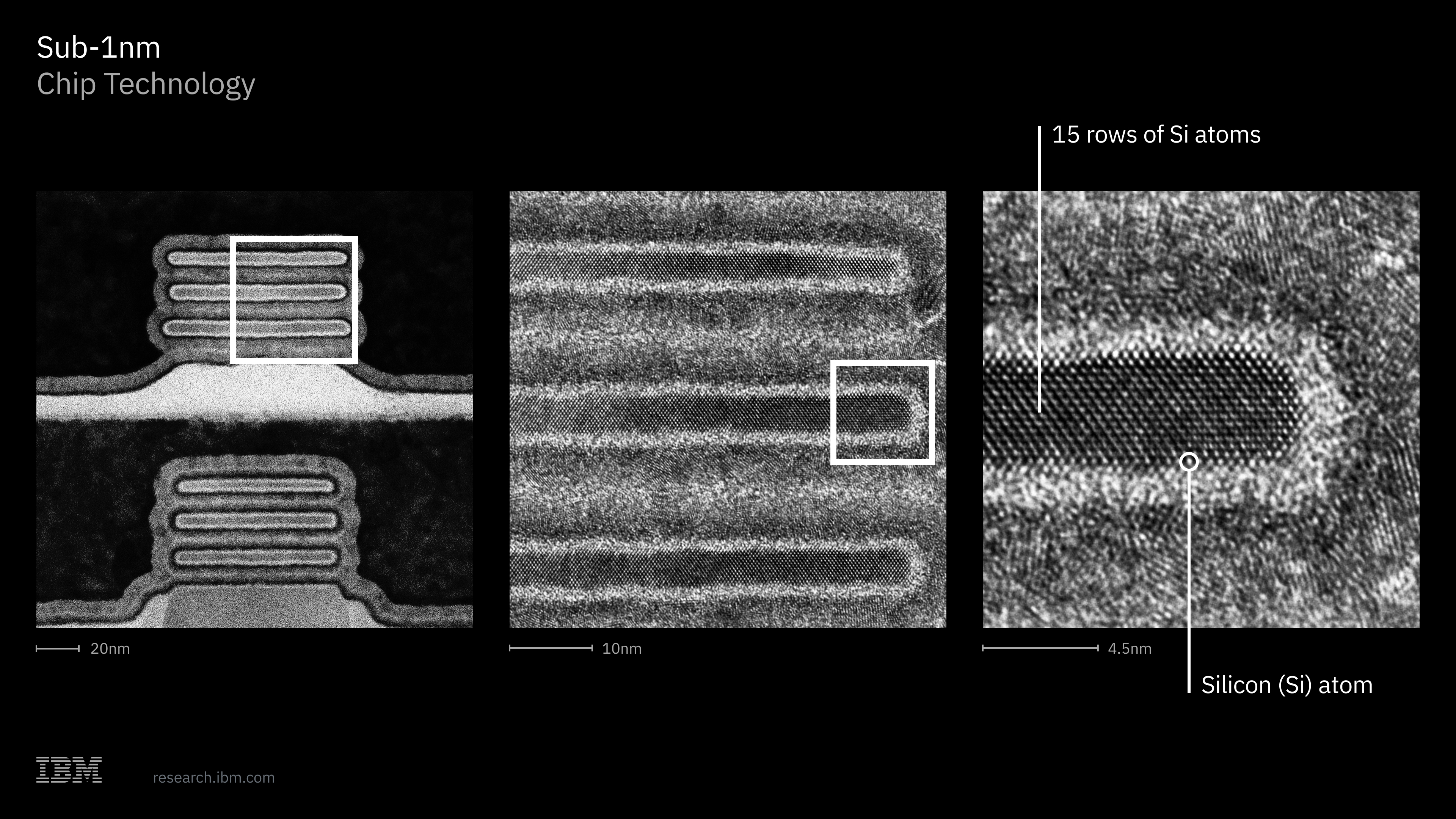
I am just astonished at the quality of the structure. Not only that, but the quality of the "cut" to then be able to take this picture. I was closely involved in EM imaging more than 30 years ago, this is just wonderful to see such pictures now.
https://sciencephotogallery.com/featured/ibm-atom-manipulati...
Doing a search on that there are loads of news articles.
But seeing progress in semiconductor nodes is always a good thing. It has felt quite stagnant these past few years.
What surprised me is that it came from IBM.
Selling a 5 nm vertically stacked chip as equivalent to 0.7 nm
Shades of Watson and other IBM lies.
also, I was expecting to see cfets mentioned.
> IBM sees a path to production in as early as the next 5 years.
5 years is a long time for a product roadmap, so there are probably some significant unsolved problems remaining, and the timeline depends on whether IBM can solve these problems.