Can you do this in a garage? Absolutely, but learn everything you need to know from an ensemble of safety-minded mentors before you strike out on your own.
It's not just about safety for you, proper disposal of these chemicals is essential for the many generations to come. Sometimes it is inexpensive, sometimes it is costly. You need to know how before you start, or it costs a lot more.
(Also, you can get someone else to pay for the hardware, the infrastructure, the material, the resists, the reagents, the safety training, and the waste disposal if you work/volunteer at a university's photolithography facility. They'll probably pay you, too.)
I needed to dissolve(ha!) fluorite once. You can get it started by adding a few drops of conc H2SO4 to your beautiful aqua regia solution. It goes deeper red, some happy bubbles appear, and as long as it stays put, makes it's own "aqua nasty"(pg88) as you gently add your powdered sample.
I thought AQR+SA was called aqua nasty, but I cant get any hits other than this AA pdf with explicit HF added. Maybe an actual chemist can chime in, is there another name for the aqua regia +H2SO4 mix?
https://archive-resources.coleparmer.com/Manual_pdfs/28750-1...
disturbing that we know this
    INHALATION

    Estimates of the lowest lethal concentrations for hydrogen fluoride range from 50-250 ppm for 5-minute exposure and are based on accidental, ***voluntary*** and occupational exposure information.
I was hoping that with 50 years of development behind us, the home fabricators could use less complex methods and less hazardous chemicals. In other words, can the folks who lived it help people like this by saying "If we had to do it over, I'd go about it like...."
Any suggestions? If you had to reboot the chip fab business on a budget what would be a more practical approach?
Yes Gordon Moore created a superfund site or two in California.
The HF monster everyone is talking about in this thread is dangerous only as a concentrated acid. It's highly soluble -- reduce it with a rainstorm or two and let it recombine to a neutral pH and you rapidly get to (literally!) toothpaste-level toxicity.
There's a VERY serious discussion to be had about the safety for a backyard chip fabricator. But the idea that this is some kind of long term pollutant (relative to much more serious issues like the cleaning solutions in your very own closet!) is pretty spun.
Edit: yeah, as the responses point out, the "superfund" sites in question are things like VOC contamination you see with any urban industry, nothing particular to semiconductor fabrication that would justify the upthread quote about contamination "for many generations to come".
If you are a scientist, and not in a sciency-y setting (lab), have a laminated clipboard stating chemical threats, electrical threats, biogenic threats, and particulate threats.
You may end up killing yourself. If you do, you did so in the name of science. Please, don't have others die because you failed to properly notify first responders of a threat.
Nasty stuff — the wisdom promoting garage stuff like this is questionable. :)
https://en.wikipedia.org/wiki/Hydrofluoric_acid#Health_and_s...
http://blogs.sciencemag.org/pipeline/archives/2008/02/26/san...
> The compound also a stronger oxidizing agent than oxygen itself, which also puts it into rare territory. That means that it can potentially go on to “burn” things that you would normally consider already burnt to hell and gone, and a practical consequence of that is that it’ll start roaring reactions with things like bricks and asbestos tile. It’s been used in the semiconductor industry to clean oxides off of surfaces, at which activity it no doubt excels.
> There’s a report from the early 1950s (in this PDF) of a one-ton spill of the stuff. It burned its way through a foot of concrete floor and chewed up another meter of sand and gravel beneath, completing a day that I’m sure no one involved ever forgot. That process, I should add, would necessarily have been accompanied by copious amounts of horribly toxic and corrosive by-products: it’s bad enough when your reagent ignites wet sand, but the clouds of hot hydrofluoric acid are your special door prize if you’re foolhardy enough to hang around and watch the fireworks
Here's a video of some French people introducing the substance to things like a rubber glove and leather:
http://blogs.sciencemag.org/pipeline/archives/2013/04/05/chl...
TL;DW: FIRE!
You first learn how to create a transistor, then basic AND/OR logic gates with individual transistors, then adders and subtractors, and then eventually a pipelined processor with look ahead execution.
Why do I say so? Because imo the most feasible form of interstellar travel is extremely slow (think a few times Voyager probe speed). Most of the technology (energy, propulsion, etc) to achieve this already exists (unlike proposals like Project Starshot), and you can take huge amounts of mass with you.
The problem is, things break down on your way. Going slow permits bringing large radiation shields (made simply of water), but the time between Star systems would still be of the order 10,000-100,000 years. Not much needs to be done on the way -- hence most circuits and mechanisms can be kept inactive -- but still you're going to have circuits and all sorts of equipment break down. There's a minimum energy expenditure needed for course correction and an associated simple but constant information processing required. So I believe you essentially need to have a way to keep fabricating chips on your way (unless you could store some reserves in a very well shielded compartment?), probably every few hundreds of years. Some elements may need recycling too. Some mechanical components e.g. propulsion systems might need periodic reconstruction/recycling also, but the technology for compact mechanical manufacturing is pretty well established -- a good machine shop with a few CNC mills, maybe some 3D printers and the like can be made to manufacture a complete propulsion system, while also having total self-fabrication capability.
There's also necessity of chips for when arriving at the destination -- again simply bringing the chips with you probably isn't viable, since it would be a while once you could establish a large modern semiconductor manufacturing plant. Again a compact fab is needed (the Starship plant itself could be used in the beginning).
Once you have those kind of capable Starships (which require some difficult but not unthinkable technology), colonizing the galaxy isn't really out of question, provided there are enough Earth-like planets (or other kinds of technologically-feasible planets) out there. You would colonize a planet and use it to build a new Starship once it were well established. Probably needing a few millenia to take over the planet and mine the needed minerals and nuclear fission fuel -- not really a big deal on our colonization time scale of 100,000s of years.
I'm also assuming this is some kind of Generation Ship, because otherwise compact self-fabrication of state of the art semiconductors may be too difficult (one of the amazing things about organic life is its amazing compact self replication). The psychological realities associated with generation ships aren't too rosy, but I think the end goal makes it acceptable (and some engineering can make them not too infernal for their occupants). Plus I find the idea of humans themselves colonizing the Stars more pleasing, but it may well turn out that AI probes will be the ones accomplishing it (if compact state of the art semiconductor fabrication becomes feasible).
https://spectrum.ieee.org/semiconductors/devices/the-high-sc...
Impressive.
I'm not sure if I should admire or condone this kind of attitude in a science related context.
I imagine flexible, thin film, large panel based semiconductor SoC. It will not be just a mere microcontroller or IoT node, but a full fleged computing form factor. Think your wall as big plastic computer.
http://www.flexolighting.eu/ (These guys have some pictures of the process).
It's probably also possible to print transistors directly. Here's a paper from 2017 that outlays that process.
It's a giant pcb and ic combined, both custom to each other and the application.
But now I have a follow up question, if getting a clean room is obviously harder, isn't "clean box" more doable? E.g., if you line up a bunch of tables, and put a long box on top that acts like a poor man's assembly line. The insides of that box are only accessible through gloves that are attached to holes on the sides of the box, and plenty of glass windows to look inside (kinda like the box in movie 'Life'). How cost effective and feasible (i.e., gets the job done) would that be compared to a clean room? maybe you could go sub-micron with it if not sub-100nm.
Using long plastic box with a 3 axis gantry inside might be doable.
https://harpers.org/archive/1998/11/the-radioactive-boy-scou...
Other challenges include smaller lithography and CMOS fabrication using a self-aligned gate process. But there are pitfalls ahead, including chemicals that can kill with in trace doses...
I fabricated my own ICs as a teen in my freshman year of college as part of our program, but that obviously wasn't at home. It was still awesome, just going through the entire process.
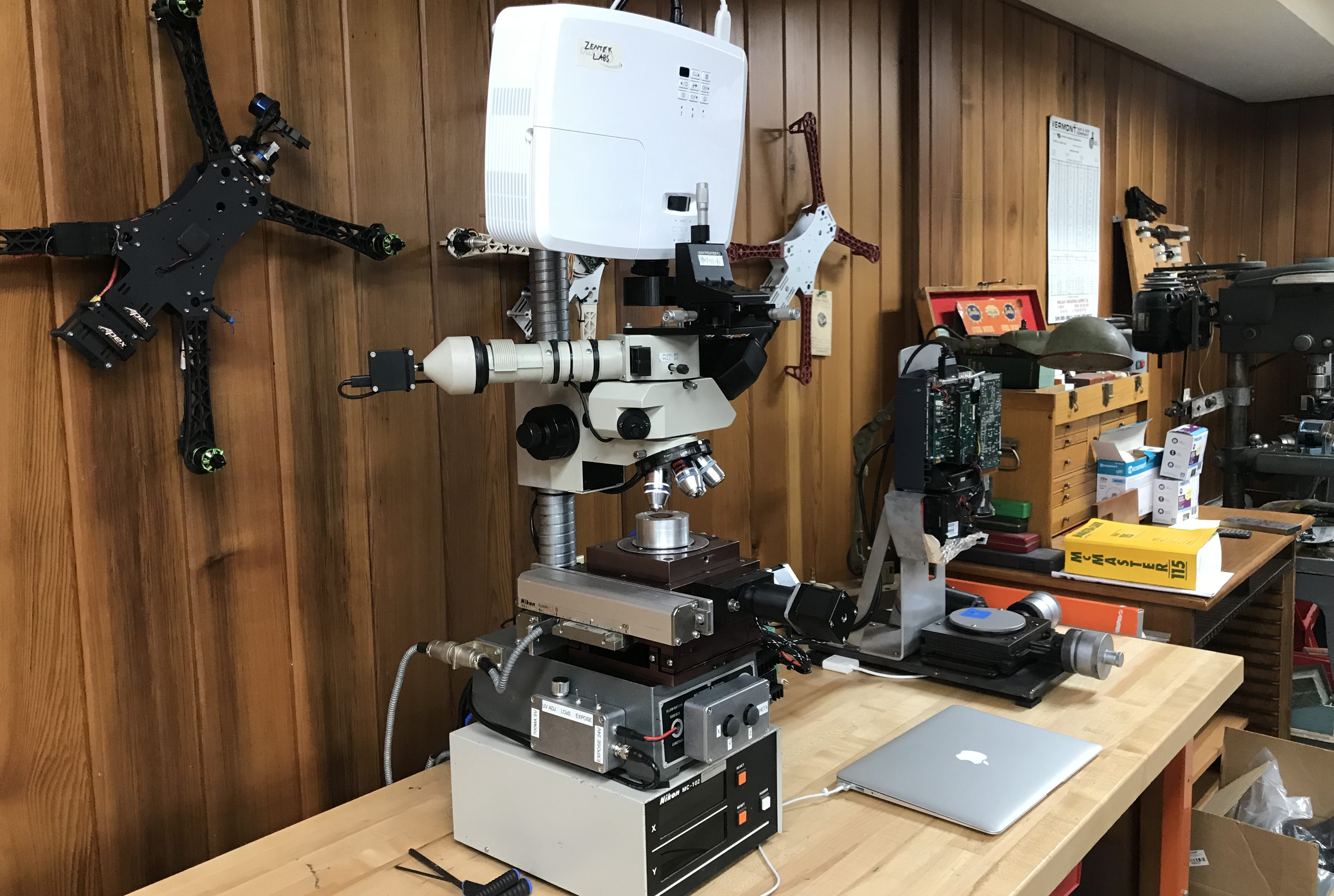
Take a tour in a home fab: https://www.youtube.com/watch?v=TrmqZ0hgAXk
His website and Youtube channel are so richly filled with knowledge that so desperately needs to be in the public domain, instead of being locked in corporate structures.
All of this information is public domain, what are you talking about? This is extremely well understood stuff.
Even with millimeter-scale components, I'd still think dust and debris could be a real problem. Is it just that 12 hour runs are short enough to just accept an imperfect production output, since it's a personal project, or is dust not as big a deal at this scale as I'd imagine?
Static electricity damage is prevented by grounding everything. (Important during lithography.)
The hard part is getting a reliable plasma oven and the requisite chemicals plus running the process to reliability.
Perhaps it can do 5um with a different resist.
There is small number of field-programmable analog array (FPAA) products and FPGA/FPAA hybrids in the market. I hope they become better and more available (never used one myself).
Not to mention, a lot of the dopants are pretty nasty too.
Maybe for you. I find silicon fabrication to be much more interesting.